
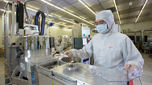
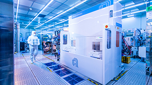
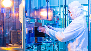
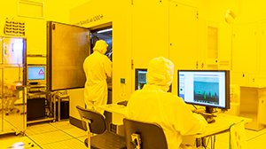
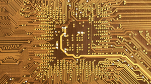
Integrated Circuit Manufacturing and Semiconductor Components
IntroductionThis course provides an overview of the development of the global semiconductor market and three Taiwanese three semiconductor sub-industry sectors, including IC design, IC manufacturing and IC packaging and testing; examines how emerging applications are driving demand for chips, touching on AI chips, automotive electronics, and wide bandgap semiconductors.
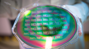
Wafer Manufacturing and Epitaxy
IntroductionEpitaxy is a method to grow or deposit monocrystalline films on a structure or surface. There are two types of epitaxy-homoepitaxy and heteroepitaxy. Homoepitaxy is a process in which a film is grown on a substrate of the same composition. Heteroepitaxy is a film that is grown on a substrate, which has a different composition. Epitaxial silicon is grown using vapor-phase epitaxy (VPE). This is a modification of chemical vapor deposition (CVD). Another technology, molecular-beam epitaxy (MBE), is mainly for compound semiconductors. MBE is a slow, line-of-sight technique, not suitable for filling trenches and other three-dimensional structures.
Oxidative Diffusion
IntroductionIn thermal oxidation, silicon wafers are oxidized in furnaces at about 1000 °C. The furnaces consist of a quartz tube in which the wafers are placed on a carrier made of quartz glass. For heating there are several heating zones and for chemical supply multiple pipes. Quartz glass has a very high melting point (above 1500 °C) and thus is applicable for high temperature processes. To avoid cracks or warping, the quartz tube is heatened slowly (e.g. +10 °C per minute). The tempering of the tube can be done very accurate via individual heating zones. Diffusion (sometimes referred to as annealing) is a thermal treatment used to move dopants, or impurities, and make dopants introduced by ion implantation electrically active. Oxidation forms a silicon oxide layer on the wafer's surface, which acts as an insulating or protective layer over it.
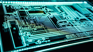
Photolithography
IntroductionPhotolithography is a patterning process in chip manufacturing. The process involves transferring a pattern from a photomask to a substrate. This is primarily done using steppers and scanners, which are equipped with optical light sources. Other forms of lithography include direct-write e-beam and nanoimprint. There are also several next-generation lithography (NGL) technologies in R&D, such as extreme ultraviolet (EUV), multi-beam e-beam and directed self-assembly (DSA). As Moore’s law has driven the semiconductor technology roadmap below 1 µm, a steady stream of new technologies has been required to produce leading-edge chips. For most of that roadmap, the enabling engineering solutions were on the processing side. For instance, the development of i-line, then KrF and ArF light sources, advanced resist chemistries, etc.
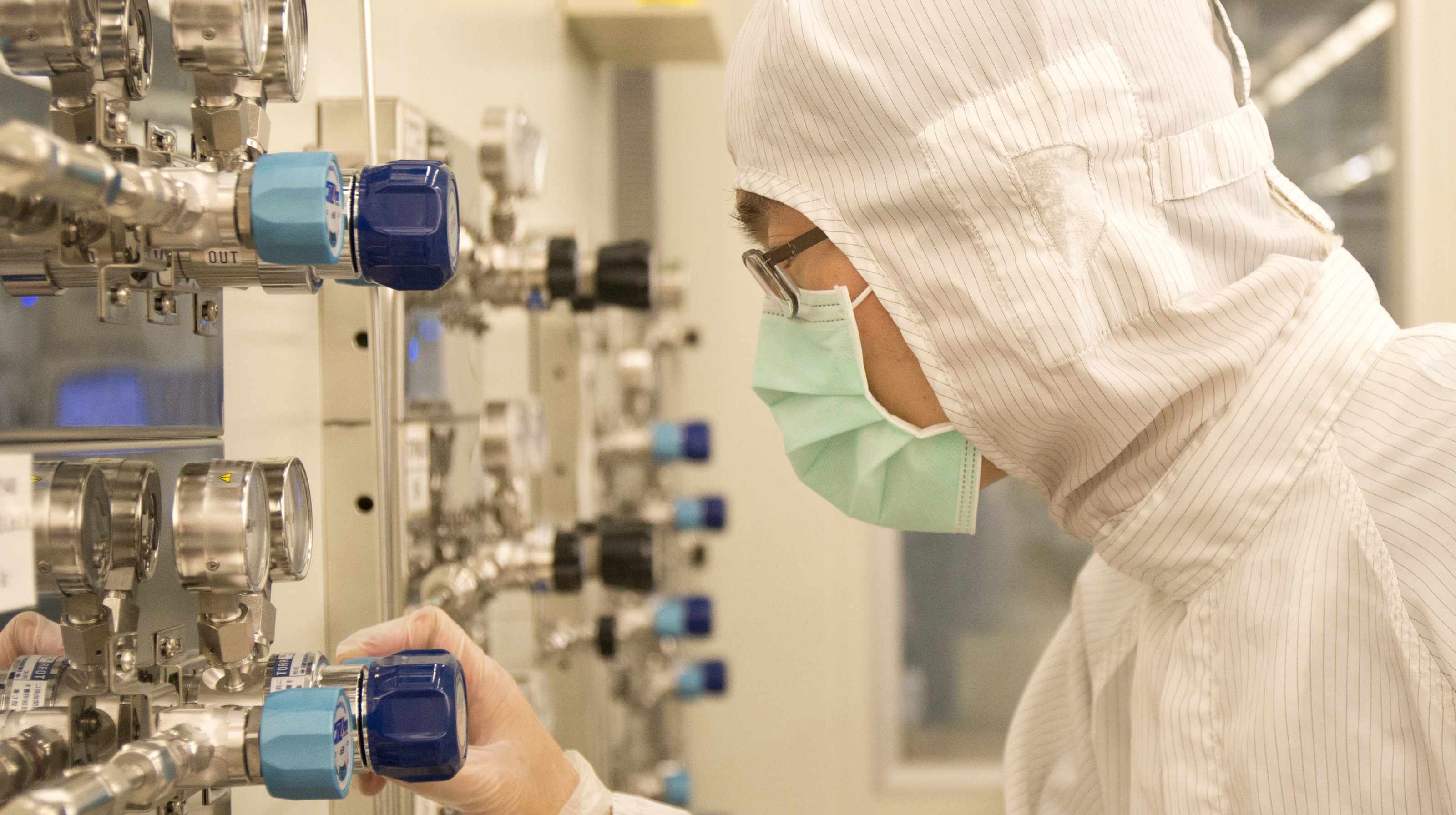
Plasma and ion implantation
IntroductionPlasma is an efficient method for many semiconductor fabrication processes. In this lesson, the basic concepts, parameters, and applications of plasma are introduced in semiconductor manufacturing field. Ion implantation is a material engineering process that charges the chemical and physical properties of solid target by driving dopants into a solid target. The history, the brief introduction of equipment, the concerns of process integrations, the applications of ion implantation are highlighted in this lesson as well. By obtaining the knowledge of plasma and ion implantation, people who attend this lesson could understand the motivations and key points of semiconductor device manufacturing by using these processes.
Etching Techniques
IntroductionIn the manufacturing of semiconductor devices, etching corresponds to any technique that removes material systematically from a thin layer on a platform (with or without preceding architecture on its interface) and leaves behind a sequence of that substance on the platform. A cover that is resistive to the etch defines the layout. Once the cover is in position, the exposed material may be etched using either "wet (chemical)" or "dry (physical)" processes.
Chemical Vapor Deposition
IntroductionChemical vapor deposition (CVD) is a vacuum deposition method used to produce high quality, and high-performance, solid materials. The process is often used in the semiconductor industry to produce thin films. In typical CVD, the wafer (substrate) is exposed to one or more volatile precursors, which react and/or decompose on the substrate surface to produce the desired deposit. Microfabrication processes widely use CVD to deposit materials in various forms, including: monocrystalline, polycrystalline, amorphous, and epitaxial.
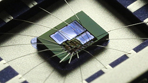
Metallization process
IntroductionConductive films provide electrical interconnection among devices as well as the outside. The primary metallization applications can be divided into three categories: gate, contact, and interconnection. Polysilicon and silicide are frequently used in gates and interconnects in MOS devices. Aluminum and copper are the metals of choice as contact and second-level interconnection to the outside. In some cases, a multiple-layer structure involving a diffusion barrier is used. Titanium / Titanium Nitride / Aluminum / Titanium Nitride is useful in providing reliable connection to external components.
Cell-based Design Concept
IntroductionThis course is designed to provide students who are using the standard component library to design digital circuit chips for the first time to quickly gain an overall understanding of the entire cell-based design process. In the future, this will help them avoid errors during the actual design process that result from only focusing on particular steps. The course not only covers the concepts of cell-based IC design flow, the standard component library, and HDL (the Hardware Description Language), it also includes the practical concepts of logic simulators, logic synthesizers, and place & route. It thus provides students with an overall understanding of software usage and design practices required for the process.
Mixed-Signal Design Concept
IntroductionThe Mixed-Signal Design Concept course focuses on the following topics: 1. advantages of mixed-signal design, 2. mixed-signal SoC design flow (including full-custom flow and cell-based design flow), 3. Verilog-top Verilog-SPICE co-design and co-simulation, 4. SPICE-top Verilog-SPICE co-design and co-Simulation, 5. mixed-signal process planning, and 6. mixed-signal design trends and challenges. The topics provide excellent insights and hints for mixed-signal IC design.
Full-custom Design Concept
IntroductionThis course is a basic introduction to full-custom IC design concepts, including basic IC concepts, full-custom IC design flow and an introduction to related software. Detailed explanations will help beginners quickly understand general CMOS process data, IC design simulation analysis and circuit layout process and skills. The course will introduce EDA software including Cadence, HSPICE and Calibre. The course also includes a CMOS overview, schematics, circuit simulation, physical layout design, layout verification (DRC, ERC, LVS, LPE) and other common design verification environments and overall processes in today’s industry. The aim is to equip students who have taken this course with the foundation and layout concepts of full-custom IC design.
CMOS MEMS IC Design Concept
IntroductionThis course will provide the beginners with a deeper understanding of CMOS MEMS from the design end to the process end. By means of TSRI's CMOS MEMS platform flow, students will have a clearer understanding of the CMOS MEMS system flow.